Research

We are interested in fundamental transport studies and device research towards more efficient electronics for computation, memory and energy conversion. We fabricate our devices at IBM Watson Research Center through collaborative joint study agreements or at National Nanofabrication User Facilities (Cornell or Harvard) and perform characterization and modeling of materials and devices in our lab. Please find below a brief description of current projects and see our publications for more details.

Phase Change Memory

Phase change memory mushroom cells in set and reset configurations.
A phase change mushroom cell in both set and reset configurations. The amorphous mushroom in the reset state increases resistance by >100x.

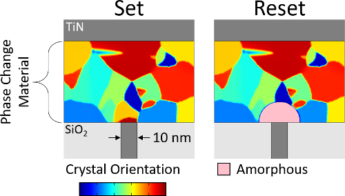
Phase change memory is a nonvolatile memory technology. It stores information as the phase of a material, that is, whether the atoms are aligned in a crystal or display no long-range order (‘amorphous’). The amorphous phase is more resistive; hence, phase can be determined by measuring resistance.

Phase change is achieved by melting and rapidly quenching the device (crystalline-to-amorphous, reset) or by heating the device to a moderate temperature and allowing it to crystallize (amorphous-to-crystalline, set).

We are interested in the characterization and modeling of materials and devices for phase-change memories, with a focus on device-level measurements of material properties and design and modeling of new phase-change elements and access devices.


Multi-contact Phase Change logic devices

Write operations in six-contact phase change logic device. With each write pulse, a toggled state is achieved. Melt and amorphous are shown in magenta and peach.

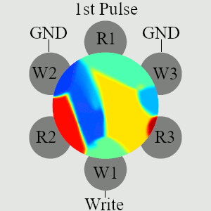
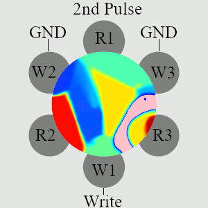
In this work, we demonstrate 2D finite element modeling of a six contact phase change device concept that can perform toggle operation through (i) isolation of read contacts due to amorphization between write contact pairs, (ii) thermal crosstalk between write contacts. There are two write paths (W1-2 and W1-3) and two read paths (R1-2 and R1-3). With the application of the first write pulse, one of the write paths (W1-3 in this case) draws a progressively larger proportion of the current and eventually melts and amorphizes, blocking the read path R1-3. Applying a subsequent write pulse, the alternative path (W1-2) draws most of the current (as W1-3 is initially amorphous) and eventually melts. As W1-2 melts, W1-3 heats above the crystallization temperature and the device cools to a toggled state (R1-3 is now blocked). With different read circuities, this device can behave as router, multiplexer, or flip-flop with smaller footprint than conventional CMOS implementation with added functionality of non-volatility.

Details of the work can be found at: https://ieeexplore.ieee.org/abstract/document/9046409


Thermoelectric transport under large temperature gradients

Double mushroom PCM cell resetting with positive polarity (positive voltage on top contact) shows clear thermoelectric effects: a mushroom forms in the top phase change layer but not the bottom.

Thermal gradients > 1 K/nm are obtained in micro and nano-structures that are self-heated to sufficiently high temperatures (such as the silicon structures we are using to study crystallization by self-heating, or phase-change memory devices). Significant thermoelectric effects arise that result in highly asymmetric temperature profiles depending on the electrical current direction. We are studying how these differ from thermoelectric effects under small gradients and how they affect operation of devices and may be utilized for improved devices.

Silicon crystallization by self-heating for large area electronics

We are investigating the possibility of achieving high-quality single crystal silicon by self-heating of patterned nanocrystalline micro or nanostructures on which high performance transistors can be built. Experimental and modeling studies of percolation transport during self-heating of the nanocrystalline silicon structures (which also apply to polycrystalline GeSbTe for phase-change memory devices).

Multi-gate silicon transistors for low power applications

Multi-gate, ultra-narrow bulk silicon transistors are investigated for very low leakage current and for studies of carrier mobility in very narrow channels. Devices are being fabricated at IBM and Synopsis Sentaurus tools are used for process and device simulations.

Light emission from zinc oxide nanorods

We have observed very intense white and blue light emission from films of ZnO nanorods under sufficient electrical bias. We are studying the optoelectronic properties of this material for potential lighting applications. Collaborative project with Alex Agrios (Environmental Engineering).

Solid-liquid phase change oscillators

We have observed large amplitude, 0.8~10 MHz self-sustained oscillations in silicon microwires due to repeated melting and re-solidification when the wires are biased through a suitable parallel capacitor and load resistor combination. We are investigating this device concept for GHz oscillators by appropriate scaling to smaller dimensions.

Instrument development

We have developed setups for high temperature characterization of electrical resistivity, Seebeck coefficient and Hall mobility of thin films. Currently, the maximum temperature is ~ 800 C (for resistivity and Seebeck, ~ 500 C for mobility).